

Specifications
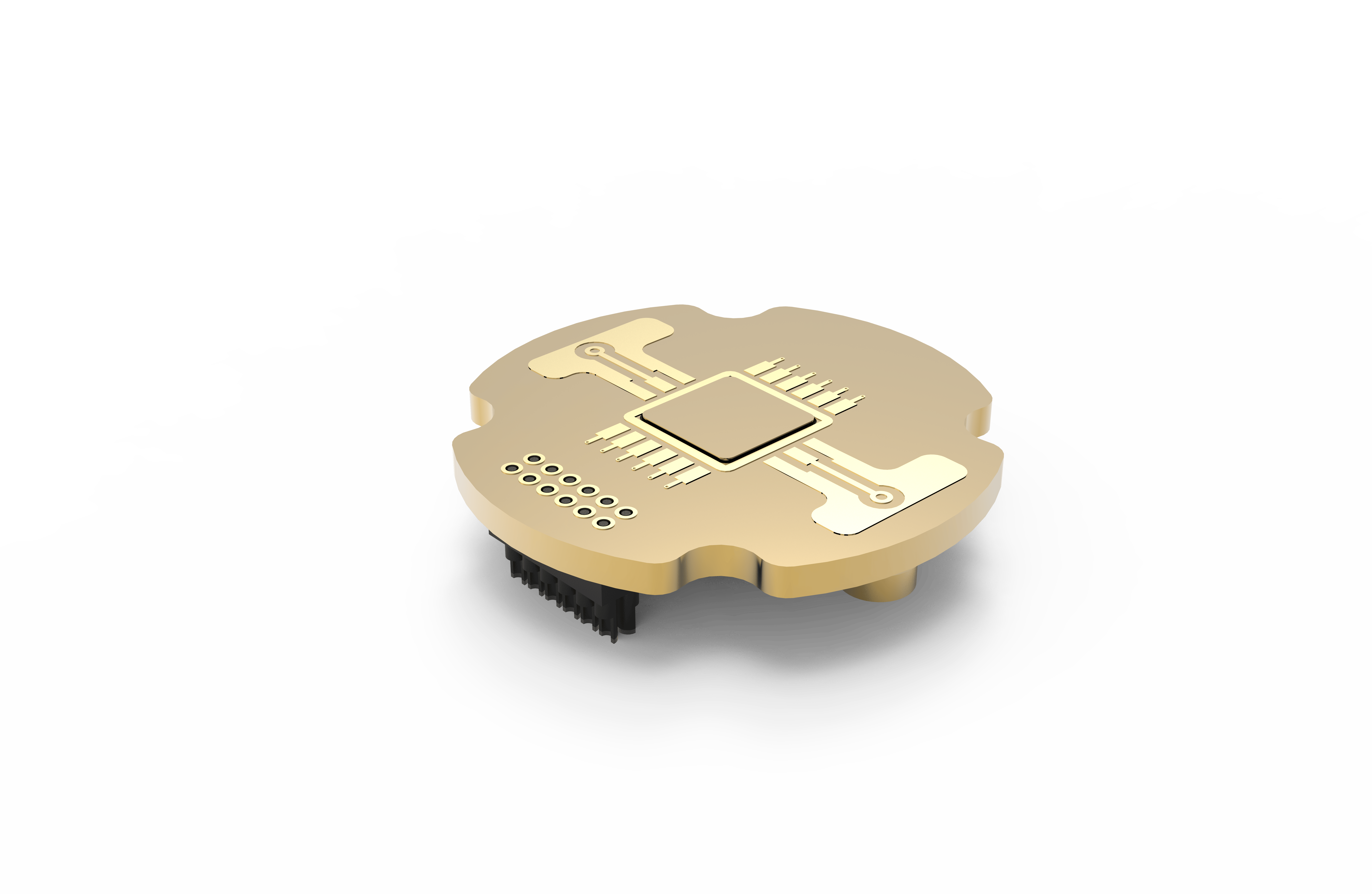
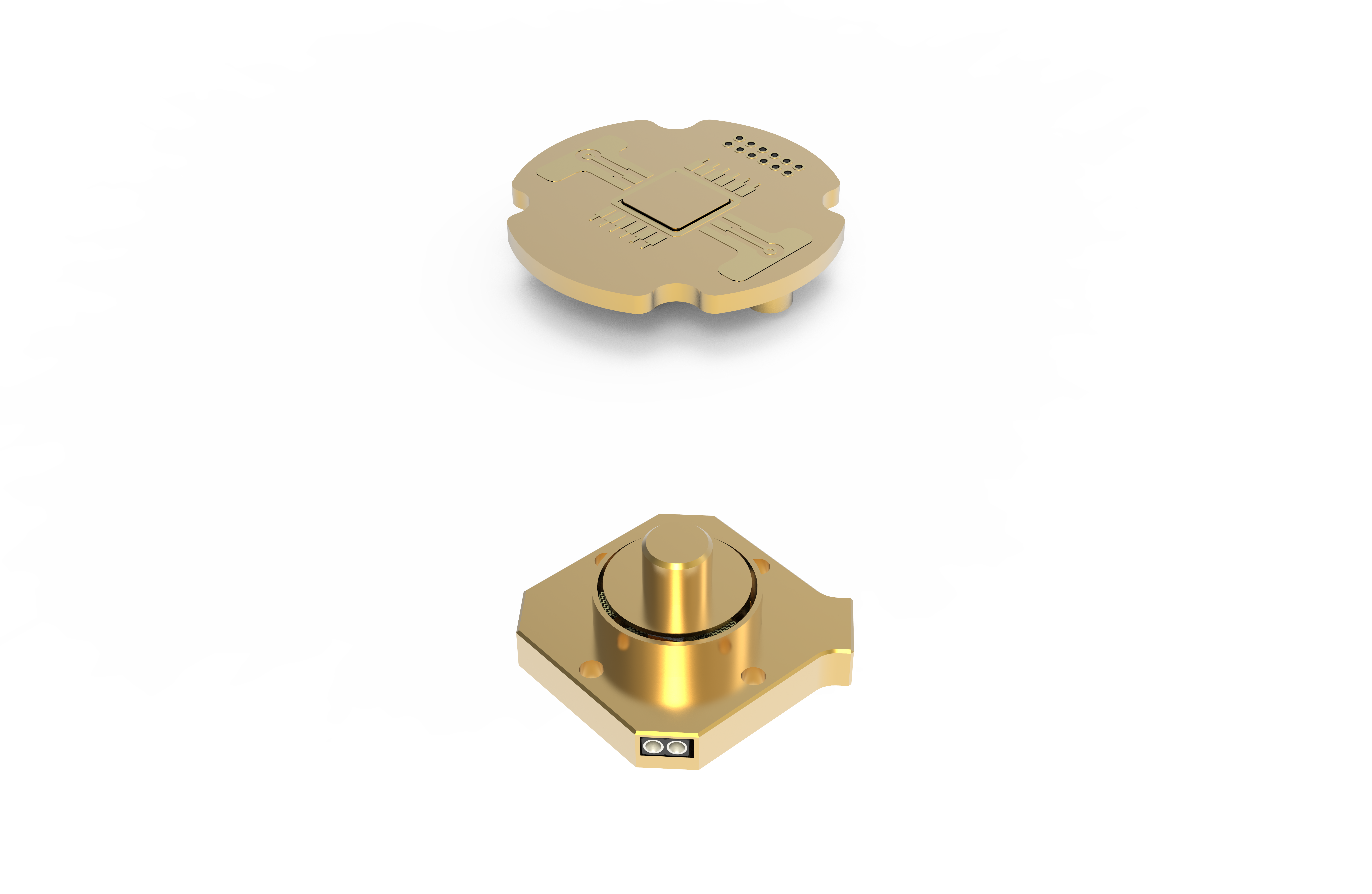
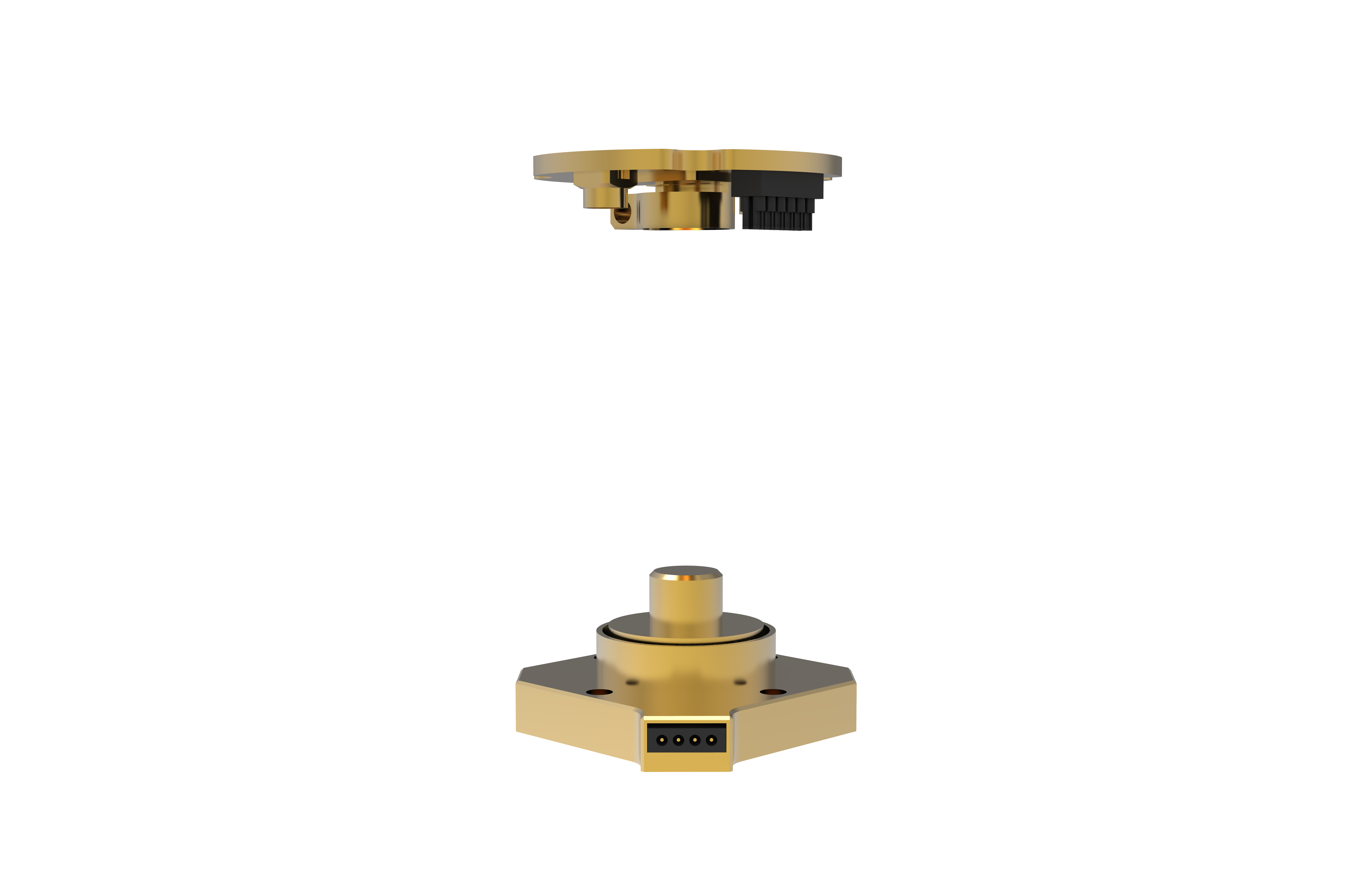
The R2D12 has 12 low-frequency DC connectors along with 2 high frequency RF (coax) connectors on a small circuit board surrounding the sample mounting platform. The circuit board is easily separated from the cryostat sample mount, providing a convenient platform for wire bonding or soldering electrical connections to the user's device. The central mounting platform utilizes quick-connect clamp for exchange boss and the 12 wire bonding pads connect via the included wiring harness.
The 2 RF bonding pads are great for coplanar waveguide studies: the signal remains shielded all the way to the device under study, ensuring a lower loss of signal. An internal copper shielding layer shields the DC lines from the RF coax to prevent signal distortion, enabling both high voltage experiments and sensitive, low signal level experiments. The sample chip is surrounded by a ground layer for additional electromagnetic shielding. The sample surface sits above the PCB height to allow for low working distance.
Maximum sample size of 6 mm square. PCB portion is reusable and replaceable with our PCB-only purchase option.